AtariBits
  • Home
  • Systems
    • 576NUC+ >
      • NUCplus4
    • 1088XEL >
      • XEL-CF Drive
      • XEL-CF3 Rapidus Variant
      • Accessories
      • XEL Archives
    • 1088XLD >
      • RGB2VGA-XLD
      • ARROW2JOY-XLD
    • CV-NUC+
  • TransKey
    • TK-II >
      • TK-II Manual
      • Installation
      • Device Compatibility
      • TK-II Archives
    • TK-II-STEREO
    • TK-II Control
  • XEP80-II
  • JOY2PIC
  • MOUSE
  • MIDI
    • MIDI 3D Printed Cases
  • UGV
    • Old UGV Archive
  • SDrive
  • RAM
  • Blog

576NUC+FujiNet Status

4/4/2021

 
Picture
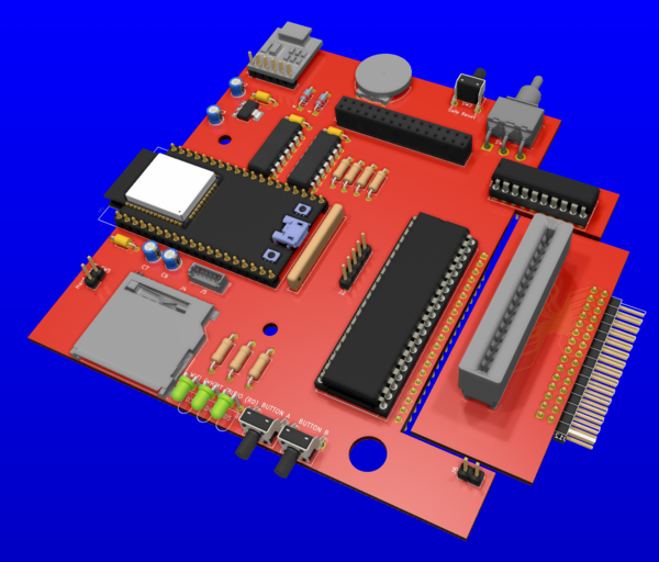
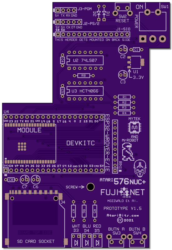
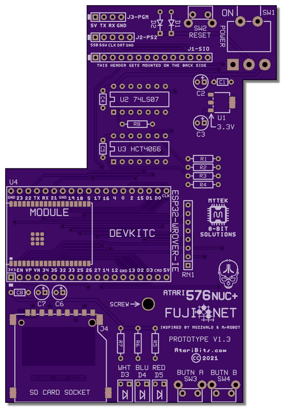
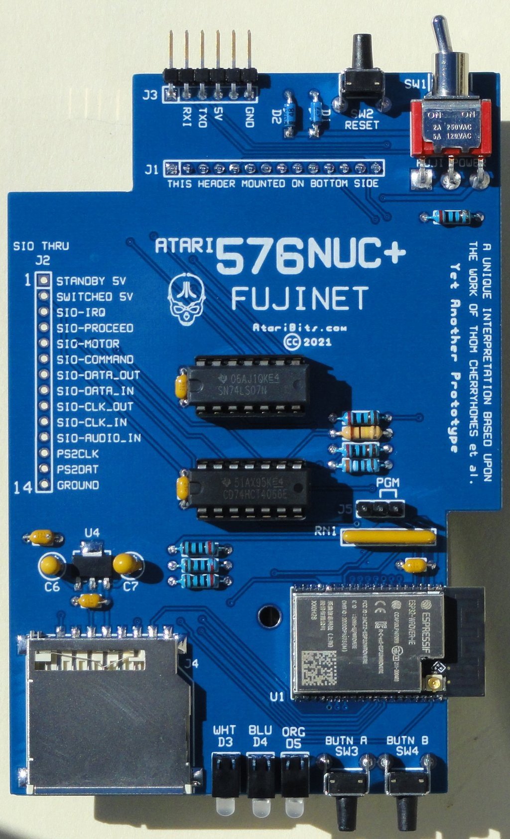
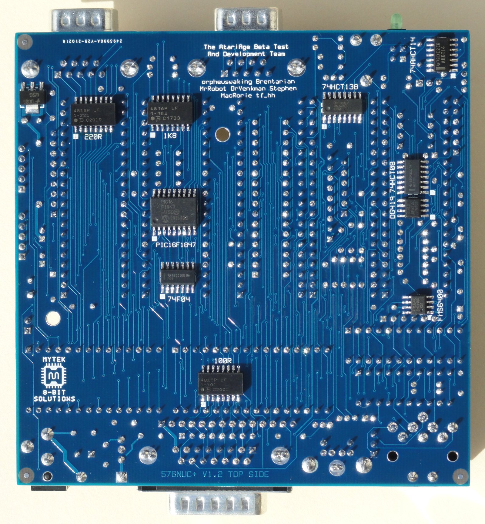
Yesterday I assembled, tested, and shipped out three prototype NUC-FujiNet V1.5 boards to people in the Beta Team for their review.

When it comes to hardware development I can be very tenacious at fine tuning the design, but I'm afraid my patience for running thorough tests of all the different aspects is quite a bit less then desired. In order to insure that all of the bugs got squished out of this particular design iteration, I'll bow out and let the Beta Team have at it (Stephen, Herb, and Simon).

Assuming that all goes well in this regard, then AtariAge member Mr Robot will finalize the production FujiNet design he has been diligently working on, which will also incorporate the option of a top side-loading cartridge slot, as well as all the interface changes coming out of the V1.5 prototype (e.g., full SIO isolation when powered off).

And thanks to AtariAge member mozzwald, the SD card detect switch feature of this design has also been fully realized in the latest firmware release, so that we can now do SD card hot plugging and/or card swapping without the necessity of powering down or resetting the FujiNet board to reinitialize the card. This is an uber cool feature!

Production Design
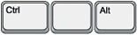
Mr Robot's production board + case design concept is rapidly advancing, as can be seen in these simulated examples he created and first posted at AtariAge. And thanks to dimensional info coming from other members in the forums, he has hopefully gotten things sized to accept any and all cartridges ever made for the Atari 8-bit, including those wider AVG and SIDE carts, and the unique XE carts with the ridge sticking out of the back side.

Picture
Picture
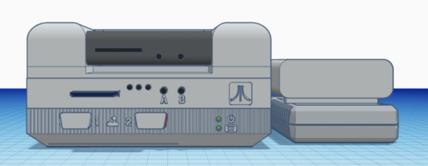
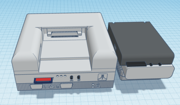
Ultimately the plan is to offer it either as a stand-alone FujiNet minus the cart connector and raised case design, or as the full boat that you see here with the cartridge port inclusive. Obviously the non-cart version will be extremely compact with a minimal height requirement, thereby having a much lower profile lid for the case.
Picture
Needless to say, I think Mr Robot's design really hit it out of the park!

- Michael

576NUC+FujiNet Prototype V1.5 coming soon

3/23/2021

 
Made several changes to the previous prototype V1.3 design, and now have another set of sample boards for testing being manufactured by JLCPCB - scheduled to arrive around the end of this week. BTW, the SD card issue I was seeing from day one, has been solved, and came down to human error as well as an incompatible SD card.

What's Changed?

The Cassette Motor Control line has now been buffered and switched out of circuit when FujiNet is powered OFF, and the SD Card Detect Switch is now being sensed by IO12 on the ESP32, and will eventually see future support in the firmware (Now Implemented in firmware version 0.5.879c407c).
Picture
576nuc-fujinet_proto_v1.5_schema.pdf
File Size: 69 kb
File Type: pdf
Download File

4/08/2021 update - voltage divider changed
4/03/2021 update - resistor R2 changed to 33K
3/25/2021 update - voltage regulator (U1) and SIP resistor (RN1) part numbers corrected


This will be my last prototype, with the design already proven out by previously modding a V1.3 board. However I simply couldn't resist putting a bit of polish on the process, and doing one last board run with all the V1.5 changes in place. I also need a few boards for others to test so as to prove out the design, so having boards that incorporated all the changes was a prerequisite.

This time around I also wanted to properly pay homage to AtariAge members Mr Robot and mozzwald. Mr Robot deserving a call out for sourcing the switches, SD socket, and LED holders. And for the direction I got from his excellent PCB layouts that came before. And of course a big acknowledgement also goes to mozzwald the creator of the hardware design being used in the standard Atari FujiNet devices, which served as both my guide and inspiration. And a shout out to the rest of the FujiNet team for a wonderful game changing innovation known simply as FujiNet (visit FujiNet.online)

So the intention is to get a few of these out to the 576NUC+ Beta Test and Development Team, and let them run it through the ringer in order to shake out any bugs. Assuming that all goes well with that, then Mr Robot will take back the reins and proceed with the final production designs. There will be more to it then just FujiNet, so keep a look out for any posts he makes concerning that.

This new SIO interface circuit which is being proven out in this final V1.5 design, has been released into the public domain, and it is hoped that it'll see future use in other FujiNet related projects.

- Michael

576NUC+ Keyboard Functions (Part 3)

3/14/2021

 
Picture
Atari Key Codes assigned to PS/2 Keys
This will wrap up the coverage on the keyboard functions, with this episode specifically digging into how the PS/2 navigation keys are mapped vs. the Atari. For the rest of the key map that has not been covered by these tutorials, you can refer to the online TK-II Manual.

Unlike a stock Atari keyboard the PS/2 keyboard has a separate section to the right of the normal keys, and to the left of the numeric keypad that moves the cursor in interesting ways.

Initially, the arrow keys mimic the same action as seen when pressing CTRL+Arrows on a stock Atari keyboard. This action can be modified by pressing the control key in combination, thus rendering the same symbol as its Atari counterpart. Or the arrow mode can be changed by momentarily pressing ALT+A which will toggle it. When toggled, it either renders the Symbol or the CTRL+Arrows equivalent depending upon its current setting.
ALT+A is a volatile setting and will revert to the normal PS/2 arrow mode when the system is powered down, and back up.
In all cases, pressing control in combination with the arrow keys will temporarily reverse the present mode. So if you press CTRL+Arrows when in the normal 'PS/2 mode', that will produce symbols instead of cursor movement. Whereas if in 'Atari mode', will result in moving the cursor, with symbols only being rendered when no control key is pressed in combination.

Using SHIFT in combination with the PS/2 arrow keys produces the same symbols as the stock Atari keyboard, no matter which arrow mode you are currently in. SHIFT+CTRL when pressed with the PS/2 arrow keys, will not produce a character but instead mimic the same key codes as produced by the stock Atari keyboard for this same combination of keys.

The Insert key when pressed by itself will insert space to the right of the cursor, and when pressed with SHIFT, will insert extra blank lines below the cursor.

The Delete key when pressed by itself will delete characters or space to the right of the cursor, and when pressed with SHIFT, will delete lines below the cursor.

Home when pressed with either SHIFT or CTRL will clear the screen and home the cursor to the upper left. When pressed alone, will invoke a 1200XL function of simply homing the cursor to the left on whatever line it was on without clearing the screen.

End will invoke a 1200XL function to move the cursor to the far left of whatever line it was on.

PgUp (Page-Up) will invoke a 1200XL function and move the cursor directly up to the top left of the screen.

PgDn (Page-Down) will invoke a 1200XL function and move the cursor to the bottom left of the screen.
Note: all the 1200XL function key codes are available in any XL or XE OS, but not the older 400/800 OS.

Those last 4 special navigation keys (Home, End, PgUp, PgDn) can be very useful when utilized in an Atari program,  especially anything that requires the user to navigate a menu. For a good example, check out the customized SDrive Control Program or AtariAge member flashjazzcat's SIDE Loader and the Uno Cart contributions. Also FJC's The Last Word makes good use of these keys.

As FujiNet continues to mature, it would be nice to see more of these  special navigation keys play a roll in navigating the TNFS directories in a similar way to the examples given above.

- Michael

576NUC+FujiNet Prototype V1.3 in Process

3/12/2021

 
Because of changes that were required in the first prototype, and then getting a bit more inspiration from a recent DIY THT build project, I decided to create a new hybrid prototype that would allow either a ESP32 SMT module or ESP32 THT DEVKITC to be utilized.
Picture
Picture
Note: Although the silk screen shows a ESP32 part number with a '-IE' suffix, the cheaper version with an '-E' suffix can be substituted instead. The only difference is that the '-IE' version has both an IPEX and PCB antenna, whereas the '-E' only has a PCB antenna. Keep in mind that the one with the IPEX connector has this selected by default, and needs to be modded to use the PCB antenna instead by moving resistor R14 to the R15 position (refer to diagram - click to enlarge).

This board is currently being manufactured by JLCPCB in China, and has an expected completion date for this coming Monday.

When I get at least one board assembled and tested, I'll be sure to post the updated schematics, as well as my observations. So far I can tell you that it incorporates the same SIO interface as its predecessor, using a 74LS07 and a 74HCT4066. This new interface has been working very well, and appears to have solved the audio noise issues.

- Michael

576NUC+FujiNet Prototype Changes

3/8/2021

 
Thanks to AtariAge member mozzwald (creator of the original FujiNet hardware), it was brought to my attention that pull-up resistors should be used on 3 of the 4 signal lines of the SD card. This article goes into more detail about that.

So today I added the resistors and once again held my breath and attempted to access the SD card on my FujiNet device - No dice still not working. It was wishful thinking that it would, but with other people's units working without pull-ups, I wasn't surprised. No matter, the pull-up resistors will still be added in my design.

Next I re-flowed the solder at the ESP32 connections, but that also failed to correct the situation. When probing the signal lines with a scope I saw no activity, and the CS line remained high, which is the normal idle state. It's almost like there's no one awake inside.

At this point I can only surmise that my ESP32 possibly has at least one I/O pin that is damaged. And since it's not easy to replace, I'll be looking at a 2nd build with a fresh board and new parts.

In the meantime I've been fine tuning the design, and moved it up to Version 1.2.

Here's the Updated Schematic (3-9-2021)
showing changes to come.
576nuc-fujinet_proto_v1.2_schema.pdf
File Size: 62 kb
File Type: pdf
Download File


Another thing I discovered, was that the information I had gotten for my USB/Serial cable was incorrect, which was why I thought I needed to swap the RX and TX pins. So that's been restored to the way it was shown in the very first schematic, matching the prototype PCB that was based upon that.

Next I really didn't like where the ADC VREF voltage divider was getting its positive voltage from (SIO), so I moved it over to the regulated 3.3V bus... EDIT: I totally misunderstood the purpose of the voltage divider. In actuality it is being used to sense voltage coming from the Atari in order to determine if it's powered ON or OFF. The voltage divider simply brings the 5V of the Atari down to a level that's safe for the ESP32 to look at by one of its ADC inputs. So I have restored the original voltage divider in my schematic and renamed the wire label as VSENSE instead of VREF. The schematic download has been updated with this change.

I also decided to reduce the size of the programming header, as well as eliminate the SIO-Thru header and only pass along the PS/2 and power related signals via a 5-pin header. The PS/2 connections are present in case I wish to develop an active Wireless USB to PS/2 converter, which is something that is definitely on my wish list.

And for the final touch, the resistor array has been expanded to include the three SD related signals, thus actively pulling them up to 3.3V.

Hopefully the next time I write about this specific FujiNet prototype it will be to discuss the successful operation of the SD card.

- Michael

576NUC+FujiNet the First THT Prototype Test

3/6/2021

 
I ran into a few snags after assembling the first mostly THT NUC FujiNet prototype. The main problem off the start was that the 3.3V regulator was intended for a 5V input which didn't bode well with our diminished power supply due to the Schottky diodes that are inline with both the USB 5V and the 576NUC+ power. Specifically I wasn't seeing a high enough voltage feeding the ESP32 module as a result.

Once that problem got resolved by spec'ing a LDO (Low Drop-Out) voltage regulator. Then the only issue remaining was that the SD Card wasn't working, and in fact it still doesn't, but that will be pushed down the road until another day. However the network side of things works great as can be seen below. I was able to quickly log-in to my WiFi router, and then added a couple of existing TNFS server addresses, subsequently I was able to download a game via the internet and run it. It was quite fun and absolutely amazing all at the same time!
Picture
PicturePL2303TA USB/Serial Cable
However the freshly assembled board did require a few more tweaks...

The series resistor for the SIO-Audio had to be increased from 470 ohms to 100K because the NUC already has a fairly high gain on that audio in port, making the SAM software speech synthesizer way too loud.

I also didn't like the look or the inconsistency of the first LEDs being used, and changed them all over to a diffused NTE version instead. Since these are very high efficiency, I was able to increase the current limiting resistors to 2K for all three of them, which matched the brightness of the dual green LED's on the NUC main board. What's also rather nice is that they all look the same when not lit, having a frosted white appearance, and best of all they are inexpensive at about 14 cents a piece.

During the initial firmware flashing I had discovered an error on which pin was designated as TX and which one was RX on the programming header. They need to be swapped. Luckily the programming cable I'm using broke out each wire independently making it easy to fix the issue, and get the ESP32 programmed (PL2303TA Cable Buy Link).

By the way, I also discovered that the program select header (PGM) was not needed, since the 'A' button works in its place.

Flashing Procedure for this Specific FujiNet Board
  1. Turn OFF FujiNet power switch.
  2. Connect USB/Serial cable between FujiNet and the computer.
  3. Press and hold the 'A' button.
  4. Turn ON the FujiNet power switch.
  5. When you see both the white and blue LEDs light up release the 'A' button.
  6. You are now ready to download the new firmware.
  7. Start the FujiNet Flashing app, and after selecting the serial port associated with the cable, press the Flash FujiNet Firmware button and let it do it's thing (this takes a while).

And finally we get to the real reason I was so keen on redesigning the SIO to ESP32 interface circuit, and that has to do with a random but very noticeable noise experienced during certain sequences in shutdown and restart that has been observed in several versions of the FujiNet hardware. Disconnection of the SIO-audio input has been integrated into the new interface design in an attempt to minimize or eliminate the problem. So far the noise hasn't been seen in the initial tests of this new prototype. Or at least I haven't experienced the right conditions that will make it reveal itself (fingers crossed).

Picture
I'm only a Proof-of-Concept Prototype, so please be kind when critiquing
Here's an updated schematic (3-7-2021) showing where things are currently at.
576nuc-fujinet_proto_v1.1_schema.pdf
File Size: 61 kb
File Type: pdf
Download File

Now all I need to do is get that pesky SD card to work.

During my troubleshooting I did a continuity check of all the connections between the SD card socket and the ESP32, but so far everything looks correct. Although I haven't entirely ruled out operator error, as in my docs may not match up with reality concerning what pins do what on the socket. The datasheet for the SD card socket I'm using is really piss poor concerning the pin definitions.
Picture
That's it for now. I'll be sure to report back in when I solve the SD card problem.

- Michael

576NUC+ New V1.2 Boards are a success!

3/4/2021

 
Well some like to say 3rd times a charm, but in my case it looks like the 4th run of boards is going to claim that prize.

The road traveled in this project was much longer than I had envisioned when I first started out, thinking this was going to be an easy and quick turn around. But as they say, all good things require time and hard work in order to accomplish, and that has certainly been the case here as well. We lost a few members of the Beta Team along the way. One because of my mishandling of what was expected, and the other because of personal issues. The drop-in FujiNet adapter board is still in the works, but I think that will get sorted out before the public release of this project. So all in all I think things have been going quite well.

And now for a look at the first assembled board straight out of the sample batch. Pretty much a 99.99% perfect fit for all of the components. Only had to leave out one By-Pass IC decoupling capacitor (lower right corner) which had a lead soldered too darn close to one of the SMT chips on the bottom side. Because of the lack of space to put it elsewhere, it will be removed from the design all together. Since the board has a good distribution of these capacitors, and being a 4-layer board with inner power planes, the loss of one decoupling capacitor is not seen as an issue.
Picture
576NUC+ V1.2 Board Top - Click to Enlarge
On this go around, all SMT ICs have been resized to SOIC proportions, thus allowing for fairly easy, although skilled hand soldering. This was done not only for my sanity, but also as a prelude to public release of the PCB gerbers for DIY. Yeah you heard that right, I will be going back on what I said and release this to the public. However this is definitely a do it at your own risk, no guarantee proposition. So I better not hear a bunch of whining about people's boards not working after they've done the assembly, since I know the board design does work when assembled properly. If you don't posses expert level soldering skills, and prior SMT experience, please steer far away from taking on this project.
Picture
576NUC+ V1.2 Board Bottom - Click to Enlarge
The schematic has been updated to reflect any last minute changes in the sample boards, and the resulting pdf has been provided for download.
576nucplus_schema_only_3-3-2021.pdf
File Size: 328 kb
File Type: pdf
Download File


The production boards will be identical to what you see above, albeit missing the by-pass capacitor that had clearance issues. The version number will stay the same, since the sample boards will remain with the beta test group members, and the change is relatively minor. Oh and that improper bottom side board ID label will get corrected as well

The Gerber files, BOM, and various flashing files for the PICs, PLDs, and OS ROM will all be released to the public in approximately 2-3 months. However a couple of people that are opting to build and sell these boards in a fully assembled and tested state will get a head start on this aspect.

- Michael

576NUC+ and FujiNet PCBs are ready to ship from China

2/23/2021

 
Just checked the JLCPCB site today, and the good news is that the boards have completed the production phase and are now awaiting pick-up by DHL.
Picture
Picture
Based on previous boards that I've gotten from them in the past, the shipping should only take 2-3 days. So if all goes well I should see them arrive no later than this Friday. Then comes the most exciting part of assembling and testing at least one of each over the weekend.

- Michael

576NUC+ FujiNet Interim Prototype

2/19/2021

 
Mr Robot had been seeing a persistent although random noise occurrence during deactivation of the FujiNet. This combined with the fact that I nor the other members of the beta test team were able to deal with the very tiny SMT parts being used on the last iteration of the NUC-FujiNet board design, set me up with a new project. This project turned into a mission about making some SIO to ESP32-WROVER interface circuit changes that had been in discussion for quite some time, hopefully solving the audio noise issue, while also creating a board that even I could assemble.
Picture
New Prototype NUC-FujiNet PCB
The reason for another PCB run in lieu of doing a point to point wired breadboard for prototyping  and proving out the changes, was that in this day and age of cheap PCBs, bread-boarding is no longer the best way to prototype designs. And although this board looks all the part of a final PCB layout, it really isn't, and only serves to hopefully advance the FujiNet interface circuit, as well as give me and others something we can actually assemble by hand, while furthering our education on how the NUC and FujiNet need to play together in the best possible way.

Why the odd shape and the bigger than needed board?
This board was patterned after the previous board designed by Mr Robot that is meant to drop into the 576NUC+, lining up the switches, LEDs and such with the front and rear panels of the custom NUC enclosures he's designed. Mimicking that previous board footprint insured that it could be used in a similar enclosure if so desired, and gave me lots of room to layout the chips and traces for a very easy routing of the PCB.

New Prototype SIO/ESP-WROVER Interface Schematic
Picture
nuc-fujinet_proto_schema.pdf
File Size: 51 kb
File Type: pdf
Download File

What has fundamentally changed in the interface circuit design, is that all SIO signals are now disconnected from the WROVER module via the the ON/OFF switch SW1, including the SIO Audio-IN. Isolation of all the WROVER digital outputs are still handled via a 74LS07 open drain hex buffer which has been retained from the previous design. However for all the WROVER inputs as well as the Audio output, they now get their isolation via a 74HCT4066 quad analog switch having all the individual analog switch enables also coming from SW1. So in all cases the SIO signals get disconnected either through the 74LS07 or the 74HCT4066 chips when SW1 is placed in it's OFF position.

Wherever possible, thru-hole components were implemented, making for a more DIY friendly assembly. Exceptions: the WROVER solderable module was retained instead of opting for a break-out version, since a few of us beta testers already had these on hand. And the SMT SD socket was also kept, although it's relatively easy to solder. Finally because there wasn't an appropriate thru-hole replacement for the USB Serial Bridge chip (CP2102N-QFN24), I opted to go with an external FTDI (USB to Serial) cable connection to facilitate WROVER programming. An even cheaper option for this cable is to be found in the PL2303TA based cables that sell for very cheap on eBay, essentially rendering a similar USB to Serial function, assuming the Prolific driver is installed (already present in most Linux distributions).

As I write this blog entry, sample boards are currently being manufactured by JLCPCB in China, and should be arriving late next week. When that happens, one board will get assembled and tested with the hopes that the new ideas it encompasses will actually work as proposed. Whatever is learned will then be applied to a final version of Mr Robot's FujiNet board.

Exciting times ahead,
- Michael

576NUC+ Keyboard Functions (Part 2)

2/7/2021

0 Comments

 
TKNUC V1.4 Firmware

Today I'll cover a bit more about the special function 'hot' keys when using the PS/2 keyboard with the NUC.

Picture
ACTION KEY(s)
Used in combination with the
following keys

Picture
SCREEN SAVER
Picture
XRAM MODE
Picture
VGATE MODE
Picture
NumLock MODE
Picture
KEY MAP SELECTION
The following functions are non-volatile in nature, meaning that whatever their last known state was, that will get retained between power-ups.

SCREENSAVER:   CTRL+ALT+S to toggle
                              ALT+S to view setting

Enables or disables the Atari 'attract' mode. When disabled (OFF) a CTR+SHIFT+A is sent once every 3 minutes to reset the attract timer. Normally this is considered a 'null' key send by the Atari OS and will be ignored.

XRAM MODE:    CTRL+ALT+X to toggle
                             ALT+X to view setting

Selects between two different extended RAM modes. Either 256KB Compy Shop, or 512KB Rambo. Compy Shop mode allows for separate CPU/Antic access to the RAM.

VGATE MODE:   CTRL+ALT+V to toggle
                             ALT+V to view setting

Toggles VGATE chip ON or OFF. When it's ON, over scan is limited to what would normally have been visible on a CRT screen, thus eliminating graphic garbage produced during certain games or demos in the bordering areas on wider screen displays (LCDs). The NUC also has an LED showing the present state of the VGATE chip, so you should see this turning ON and OFF depending upon the last setting.

NumLock:         CTRL+ALT+NumLock to toggle
                             ALT+NumLock to view setting

This toggles the power-up state for NumLock, which determines if the numeric keypad will either be in number mode or navigation.

Pressing the NumLock key without ALT, simply toggles the mode without saving or changing the power-up state.

Key Map:           CTRL+ALT+F4 to select
                             ALT+F4 to view setting

There are 4 key maps that can be selected.
  1. US  (United States)
  2. DE  (Germany & Austria)
  3. UK  (United Kingdom)
  4. A8  (Requires re-labeled ISO keyboard)
Each time the CTRL+ALT+F4 combination is pressed the next selection in line will be chosen, and when it gets to the end, it'll go back to the first one on the list. For more information on each map selection go HERE.

- Michael
0 Comments
<<Previous
Forward>>

    Author

    My name is Michael St. Pierre and in the early 90's I decided to create my very first Atari 8-Bit upgrade. It was called TransKey.
    ---Then soon after Atari folded and I left the scene ---
    25 years later I came back with a mission to improve upon what I had started so long ago.

    Archives

    October 2025
    May 2025
    March 2025
    January 2025
    December 2024
    September 2024
    August 2024
    July 2024
    May 2024
    April 2024
    February 2024
    January 2024
    December 2023
    November 2023
    August 2023
    June 2023
    May 2023
    March 2023
    January 2023
    December 2022
    August 2022
    May 2022
    April 2022
    December 2021
    October 2021
    July 2021
    June 2021
    May 2021
    April 2021
    March 2021
    February 2021
    January 2021

    Categories

    All
    576NUC+
    AtariBits News
    C64
    ColecoVision
    Industrial Applications
    Intro
    MIDI
    Monster 600XL
    Multi-Carts
    Multi-SLOT 1200XL
    NUCplus4 Assembly
    Transkey
    XEP80-II

    RSS Feed

Powered by Create your own unique website with customizable templates.