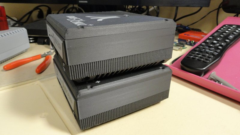
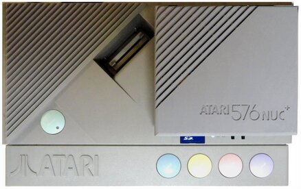
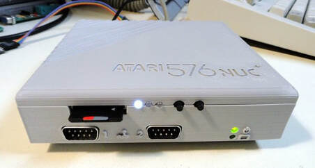
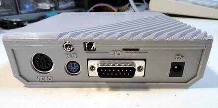
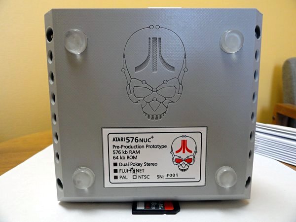
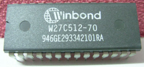
Final case design completed for 576NUCplus4 project.

Printed on Bambu Lab A1 mini PLA Matte Charcoal (11101), PLA Basic Gray (10103)

Created and Modified in TinkerCad

The original 576NUC+ case design was created by Steve Boswell (AtariAge: Mr Robot) who later released the STLs to the open source community, which I was able to modify to suit this new incarnation. This was also made possible through the use of a free online 3D CAD application called TinkerCad, a simple to use but very powerful 3D design tool.
New 3D Printer
I recently graduated to the Bambu Lab A1 mini 3D printer, and can now do some seriously good prints.
Previously I had been using an AnyCubic Kobra Plus that I picked up for ultra cheap as a customer return via eBay. It was good for getting my feet wet in 3D printing, but I got tired of constantly having to tweak all the settings in order to get good prints, and quite frankly the Bambu blows it away. And now I can do multi-color printing the easy way.
So the cases you see above are of my final design made on the Bambu printer.
3D Printing Station Update
I had to do some rearranging to make things fit into the allocated 3D printing station space in my shop, but in the end I think it came out quite well. And I also got serious with my filament storage, opting to use sealed containers with desiccant packs inside.

Click on Image to Enlarge
 | Multi-Color Filament Changes not Good for Every Situation Although the Bambu Lab A1 mini does a phenomenal job doing the 2 color printing for the LID and the front BADGE, it wasn't able to do the same for the small lower front panel text and symbols. And when I tried, it created an awful lot of poop! Yep you heard that right 'poop', the term generally used for the filament blob that gets ejected by the printer when doing filament color changes. And boy was it proficient at doing this when attempting a different color in a vertical plane. So for that situation I resorted to using Sharpie's Silver Metallic marker, which rendered excellent results, while being very quick and easy to do. I got my markers as a 4-pack from Staples for a very reasonable price. |
 EverBilt 158 724
 HeatSets are Out
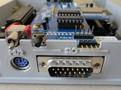
In the previous 576NUC+ case design, the upper and lower halves depended upon heat set threaded brass inserts for the screws to screw into. However I wasn't thrilled about using these since they are very dependent upon correct insertion to avoid cross-threading issues. So in this new case design I've gone with screws and nuts, with both being recessed into the case halves, and black in color to make them virtually invisible.
I sourced these from McMaster-Carr, but probably something equivalent could be gotten at your local hardware store, not requiring a minimum purchase of 100.
P/N 91249A618 Black-Oxide 18-8 Stainless Steel Pan Head Phillips Screw, 4-40 thread, 1-3/4" long, pack of 100
P/N 90328A101 Black-Oxide Zinc-Plated Steel Locknut, 4-40 thread, pack of 100
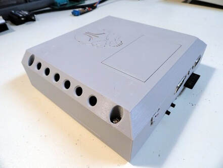
Got Feet?
On the bottom of the case there are 4 circles showing the location of the rubber feet (Clear Vinyl actually). These reference circles were sized at exactly the same diameter as the feet produced by EverBilt which can be purchased either from Amazon or Home Depot.
P/N 158 724 1/2 in. Self-Adhesive Vinyl Surface Bumpers, 16-Pack
- Michael
Previous Post


 RSS Feed
