Normally if this were a stock Atari 8-bit computer I'd say go with the modern plug 'n' play PokeyMAX in place of the original Pokey chip. However there are two reasons that won't fly on the NUC, one being an incompatibility with the TK-II chip responsible for keyboard input, and secondly there were some clearance issues. Because the 576NUC+ is an extremely condensed version of an A8, there simply isn't a lot of room between chips and other required hardware. And due to a wider footprint of the PokeyMAX vs. the Atari Pokey chip, this presents problems, one being a standoff for the FujiNet daughter board getting in the way.
So not being one to throw in the towel when the going gets tough, I started looking at some of the old school solutions, namely Gumby as originally proposed by Chuck Steinman of Dataque fame. In his proposal he outlined a method of stacking two Pokey chips and then adding a circuit for address decoding to let them share space. Here's a link to the article he wrote in December 1989 about doing that very thing. What Chuck really accomplished back then, was to create the standard for dual Pokey addressing that lives on to this day, over 30 years after its initial development.
In Chuck's design he uses a single gate from an inverter chip to invert the A4 address line for connection to the original 'left' channel Pokey chip's CS1 pin, and then simply routes the non-inverted A4 address to the same pin on the stacked 'right' channel Pokey. This gives a flip-flop action between which Pokey chip is enabled, dependent upon the state of A4. To finish off the circuit, the 'right' channel audio output was handled in a pretty simple way with the addition of a single resistor and capacitor, using trim pots to balance the stereo output between channels.
Looking at the original Atari 8-bit circuit, a pull-up resistor was connected to CS1 creating a high (logic 1) on that pin, which can be easily overridden by external logic. Unfortunately I didn't do that in the 576NUC+ design, so for my upgrade that pin needs to be lifted.
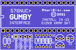
In my design I wanted to match the characteristics of the already present 'left' channel audio circuit in the NUC, thus having the same output level in both channels and eliminating the need for any trim pots. I also had to keep what I'll call the Gumby Interface circuit relatively small, due to the lack of space in the NUC. So for the A4 inversion I was able to use two resistors and a 2N7000 N-Channel FET.
Next decision was where to locate the circuit board in order to avoid a point-to-point wiring mess of the required components dangling in mid-air. And because there was a limited amount of free space available, I chose to create an XRAM piggyback PCB to give both a secure and stable mounting platform, as well as to pick up power, ground, and the A4 signal.
Note: XRAM is my abbreviation for eXtended RAM.
|
For full details on what was truly involved to bring this into reality,take a look at this schematic... |
| ||||
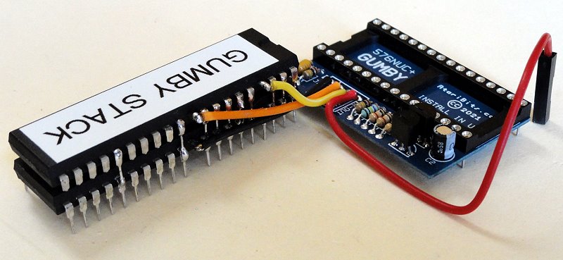
 Stacked Pokey Chips and Gumby Interface Board Connected (red wire feeds right channel audio to DIN-8 Jack)
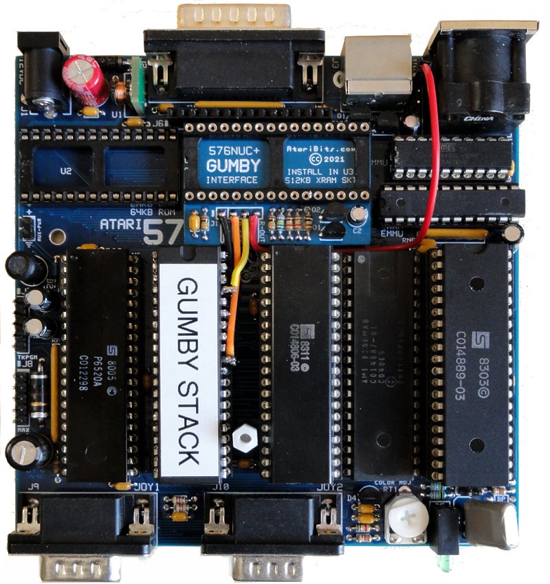
 Here's how it looks installed in the 576NUC+ (the system ROM and 512KB SRAM have yet to be inserted). It turned out pretty clean if I do say so myself.

Oh just to be perfectly clear... this project is purely a personal pursuit and will not see a public release for the gerber files, or ever get produced by someone like The Brewing Academy.
- Michael


 RSS Feed
