|
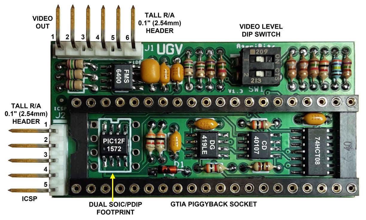
UGV Ultimate Gated Video Board
Back in the days of CRT TV's the visible image was cropped by what was called 'over scan' wrapped around the edges of the CRT picture tube. Later when computer monitors got cheaper, more people starting using them instead of their TV's. The side effect of this transition resulted in less of the over scan image being chopped off. To this day the trend has continued with the advent of modern HDTV's, which now display every bit of possible video coming out of the Atari 8-bit. As a result, some games and applications that take advantage of this normally 'hidden' area of the screen to hide various graphics manipulations (akin to racing the beam), now have all these unsightly artifacts revealed. So the main idea behind the UGV board is to hide these areas that were never meant to be seen, by 'blacking' them out. As part of its operation it also incorporates an entirely new HQ Video Driver Circuit with both composite and S-Video output quality being similar to what is seen in the UAV board created by AtariAge member Bryan. The UGV board is meant to piggyback the existing GTIA chip Atari P/N: CO14805 [NTSC] or CO14889 [PAL], thus providing a 'no solder' installation in the XL series machines. XE systems will require de-soldering the GTIA chip and installing a 40 pin socket, or in the case of the 400/800 the UGV board will get soldered directly in place of the GTIA chip. |
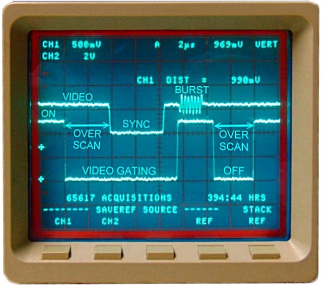
O-Scope showing Video Gate signal vs. Video Output
|
|
Microchip PIC V-Gate Timing Generator... |
|
|
Precise timing of the video gating aspect is performed by an embedded PIC MCU clocked by the GTIA's OSC pin, and then boosted by a factor of 4x by an internal PLL. This synced high speed clock makes it possible to execute code in the PIC chip quickly enough to allow gating of the video signal at just the right moment in order to eliminate over scan by switching off the Luma and Chroma before subsequently being buffered and sent to the video outputs. This gating can be disabled by bringing the PDAT pin to ground (Vss), and with no connection, a +5V pull-up resistor on this pin defaults to an enabled state. Or in other words turns it ON.
Either a PDIP or SOIC device can be used as the MCU, programmed via the ICSP header (J2), or if it is a PDIP device it can be socketed and programmed externally if so desired. However use of the PDIP package will require an additional stacked 40 pin IC socket in order for the bottom of the GTIA chip to clear the top of the PIC. |
Due to global supply shortages these chips may be out of stock at most traditional sources. However I had good luck sourcing the PIC12F1572-I/SN in a SOIC-8 package from AliExpress. |
Simple But Effective HQ Video...
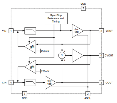 FMS6400 Block Diagram
The basis of the video driver circuit is the FMS6400 a Dual Channel Y/C Video Driver and Composite Video Summer IC chip. Basically you just feed it the proper level of the Luma 'Y' following a resistor DAC in our case, and the Chroma 'C' to get fully DC restored and filtered 75 ohm impedance video out the other end. At the same time a 3rd buffered output sums the 'Yin' and the 'Cin' to create an independent composite 75 ohm impedance video output. Since the input side of the FMS6400 is at a relatively high impedance, it eliminates the need for additional emitter follower transistor circuits and greatly simplifies the overall design of the video circuit as compared to what Atari did.
To insure that the minimum amount of noise gets introduced in this process, the FMS6400 is used in its 0 db gain mode, while the resistor DAC is composed of very low ohm values driven by a 74HCT08 Quad 'AND' Gate having much higher drive current than the CD4050 buffer chip used in the original Atari video circuit.
Using the low ohm (low impedance) resistors for the DAC's ladder makes them far less susceptible to picking up switching noise from the immediate area. The overall result produces very clean noise-free video while keeping the signal paths simple and direct.
Although the FMS6400 is an obsolete chip, it really does such a superb job for this application that it's worth buying NOS from the likes of eBay or AliExpress. And it's readily available from those sources, being sold at a very reasonable cost of less than $1.00 each (that price includes shipping when purchased in lots of 5 pieces or more). It's commonly sold as FMS6400, FMS6400CS, FMS6400CS1 which are all essentially the same part.
NTSC Users: One Simple Modification Required on the Atari Motherboard...
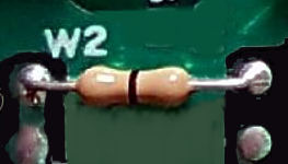 W2 Jumper
Atari for reasons I have yet to discover, decided to put a jumper from the primary crystal oscillator's output over to GTIA's PAL Color Burst Input (pin 16). On an NTSC machine this jumper is normally installed, which is bad news for the PAL detection input on the V-Gate chip. What it means is that the V-Gate chip will think it's in a PAL machine even though it's actually an NTSC. This will have the end result of causing a blue vertical stripe on the left side of the screen, and a red stripe on the right side whenever V-Gate is enabled.
The fix is easy, and amounts to either cutting one lead on the jumper or removing it all together. in either case the jumper was never required, and there will be no detrimental effect to leave it out permanently.
On all XL and XE systems it's identified as 'W2' on the motherboard's silk screen, and is either located close to the main oscillator and crystal on an XL unit, or close to the unpopulated PAL Color Burst oscillator circuit where the 74LS74 would normally be located if it were an XE PAL machine. The 74LS74 is designated as U21 on the 65XE and 130XE, or as U10 on an XEGS.
The 1200XL is the exception to this rule, and although it too has a place for a jumper (designated as 'W10' instead), it apparently was never installed in most, or maybe all of those machines. So no modification is likely to be needed. And lastly the 400/800 series didn't even have a jumper and left the NTSC GTIA pin 16 unconnected, which is what we want.
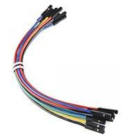 Female to Female Jumper Wires
Installation: 600-1200XL is Extremely Easy and Virtually Solder-less..
When a fully assembled board is piggybacked with the Atari's GTIA chip, the UGV instantly becomes a fully functional device with minimal external connections required other than the video outputs. Which in most cases consists of a couple of soldered points on the Atari motherboard in order to feed the stock 5-pin DIN A/V jack (reference TBA's UAV manual for locations).
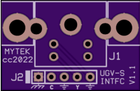
And for those that wish to have an industry standard S-Video Mini-DIN connection, there's also an optional solder-less interface board available that enables a simple plug-in interconnection utilizing pre-made off the shelf jumper wires (check out the BOM for a source of these).
When a fully assembled board is piggybacked with the Atari's GTIA chip, the UGV instantly becomes a fully functional device with minimal external connections required other than the video outputs. Which in most cases consists of a couple of soldered points on the Atari motherboard in order to feed the stock 5-pin DIN A/V jack (reference TBA's UAV manual for locations).
And for those that wish to have an industry standard S-Video Mini-DIN connection, there's also an optional solder-less interface board available that enables a simple plug-in interconnection utilizing pre-made off the shelf jumper wires (check out the BOM for a source of these).
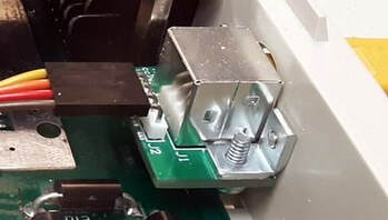
Installation: XE/XEGS/400/800 Not so Simple, Requiring Soldering & De-soldering Skills...
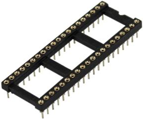
The XE line of computers never had the IC chips socketed (might also apply to certain 600/800XL systems), and thus will require desoldering of the GTIA chip and installation of a 40 pin IC socket in its place. This IC socket should preferably be a machine pin type as shown in the image below.
IC Socket Suggested Vendors and Part Numbers...
Jameco Part no.: 41136
Digi-Key Part no.: ED3032-ND
Mouser Part No.: 575-1104764041001000
400/800 Special Considerations: Even though the UGV utilizes a low profile piggyback design, the 400/800 computers have such severe space constraints due to the cast aluminum RF shielding surrounding the plug-in cards, that the GTIA's socket needs to be removed (de-soldered). After doing so, the UGV board needs to get soldered directly in its place, and then plug the GTIA chip into the UGV's socket instead.
Also the ICSP header (J2) on the UGV needs to be left off the board assembly when dealing with the older style 400/800 6502 CPU Card because of additional interference problems with the edge card connector where the board gets plugged in. This will require making a temporary connection when doing ICSP flashing of the on board SMD V-Gate PIC chip. However if your UGV board is using a socketed THT version of this chip, it can be removed and flashed out of circuit.
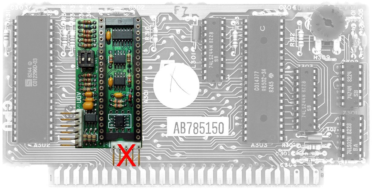 UGV on 400/800 6502 CPU Card (later SALLY version has GTIA on far left)
In addition to removing header J2, the later SALLY CPU Cards will also require that the UGV video connection header J1* gets removed as well, thus requiring the video output signal connecting wires to be directly soldered to the header pads instead.
*Note: on the Sally CPU Cards the GTIA chip is mounted on the extreme left side of the board. Putting it real close to the aluminum RF shield on that side, and not allowing for anything on the UGV board to stick out much beyond the CPU Card itself.
*Note: on the Sally CPU Cards the GTIA chip is mounted on the extreme left side of the board. Putting it real close to the aluminum RF shield on that side, and not allowing for anything on the UGV board to stick out much beyond the CPU Card itself.
|
This is Meant to Replace Your Stock Atari Video...
Due to a non-buffered color connection to GTIA, the stock video will not look good with the UGV installed, and especially if the VGATE function is enabled. Therefore it is meant to entirely replace the stock video coming out of your Atari. Since the UGV is all about getting High Quality video output, there is no real sacrifice in no longer using the original stock video circuits. In fact it just makes good sense to cut loose the original video connections going to the A/V jack, and instead route the UGV video outputs to that same jack. The Brewing Academy has an installation pdf manual for their UAV product that does a good job of showing how to eliminate the connection of the A/V jack to the stock video, and then take it over for the UAV. This same method will also work for the UGV. |
|


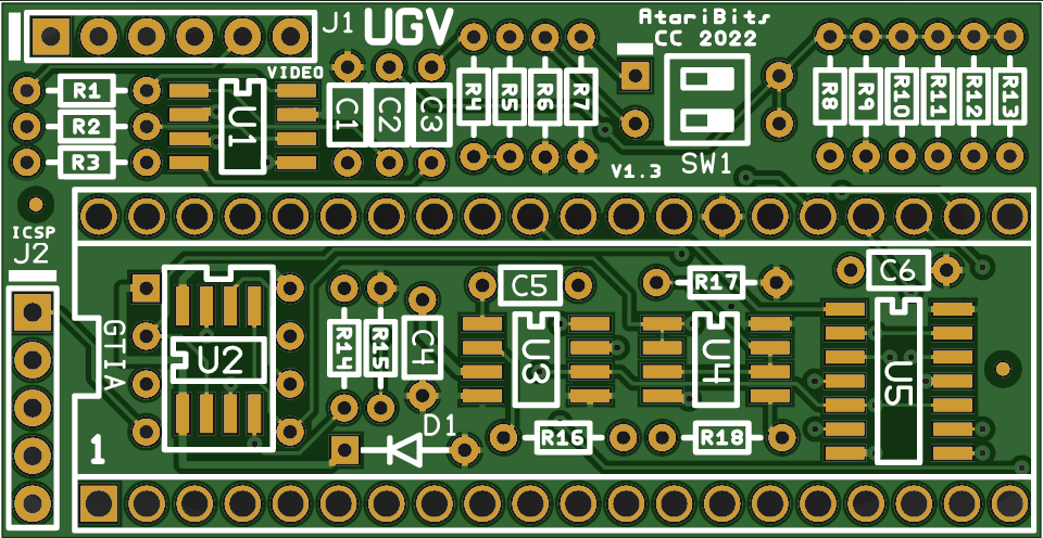
Build It / Flash It / Use It
NEW UGV Video Board
NOTE: The Value of R16 was Updated on 3/5/2023
|
Header J1 - Video Output 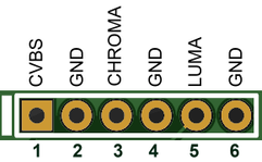
CVBS = Composite Video Blanking & Sync
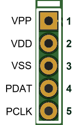
Header J2 - ICSP
If the RF Channel Select switch on the Atari is no longer needed, it can be used to disable and enable V-Gate when connected to PDAT. DipSwitch SW1 - Video Data Level Adjustment 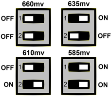
Allows adjustment for video converters. 660mv is the Standard Video Output Level, bringing it just a tad under 1 Vpp when the Sync gets added back into the equation. | ||||||||||||||

|
Click Image to Enlarge
| |||||
