Mr Robot had been seeing a persistent although random noise occurrence during deactivation of the FujiNet. This combined with the fact that I nor the other members of the beta test team were able to deal with the very tiny SMT parts being used on the last iteration of the NUC-FujiNet board design, set me up with a new project. This project turned into a mission about making some SIO to ESP32-WROVER interface circuit changes that had been in discussion for quite some time, hopefully solving the audio noise issue, while also creating a board that even I could assemble.
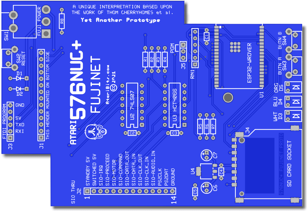
New Prototype NUC-FujiNet PCB
The reason for another PCB run in lieu of doing a point to point wired breadboard for prototyping and proving out the changes, was that in this day and age of cheap PCBs, bread-boarding is no longer the best way to prototype designs. And although this board looks all the part of a final PCB layout, it really isn't, and only serves to hopefully advance the FujiNet interface circuit, as well as give me and others something we can actually assemble by hand, while furthering our education on how the NUC and FujiNet need to play together in the best possible way.
Why the odd shape and the bigger than needed board?
This board was patterned after the previous board designed by Mr Robot that is meant to drop into the 576NUC+, lining up the switches, LEDs and such with the front and rear panels of the custom NUC enclosures he's designed. Mimicking that previous board footprint insured that it could be used in a similar enclosure if so desired, and gave me lots of room to layout the chips and traces for a very easy routing of the PCB.
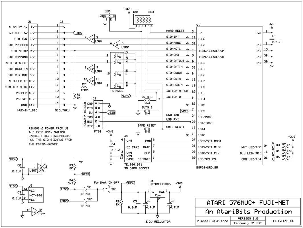
New Prototype SIO/ESP-WROVER Interface Schematic
| nuc-fujinet_proto_schema.pdf |
What has fundamentally changed in the interface circuit design, is that all SIO signals are now disconnected from the WROVER module via the the ON/OFF switch SW1, including the SIO Audio-IN. Isolation of all the WROVER digital outputs are still handled via a 74LS07 open drain hex buffer which has been retained from the previous design. However for all the WROVER inputs as well as the Audio output, they now get their isolation via a 74HCT4066 quad analog switch having all the individual analog switch enables also coming from SW1. So in all cases the SIO signals get disconnected either through the 74LS07 or the 74HCT4066 chips when SW1 is placed in it's OFF position.
Wherever possible, thru-hole components were implemented, making for a more DIY friendly assembly. Exceptions: the WROVER solderable module was retained instead of opting for a break-out version, since a few of us beta testers already had these on hand. And the SMT SD socket was also kept, although it's relatively easy to solder. Finally because there wasn't an appropriate thru-hole replacement for the USB Serial Bridge chip (CP2102N-QFN24), I opted to go with an external FTDI (USB to Serial) cable connection to facilitate WROVER programming. An even cheaper option for this cable is to be found in the PL2303TA based cables that sell for very cheap on eBay, essentially rendering a similar USB to Serial function, assuming the Prolific driver is installed (already present in most Linux distributions).
As I write this blog entry, sample boards are currently being manufactured by JLCPCB in China, and should be arriving late next week. When that happens, one board will get assembled and tested with the hopes that the new ideas it encompasses will actually work as proposed. Whatever is learned will then be applied to a final version of Mr Robot's FujiNet board.
Exciting times ahead,
- Michael
 RSS Feed
