The addition of the extra AV jacks will facilitate all of the input possibilities that come with the A/V-to-HDMI converter. So now not only will the 80 column output be sent over HDMI, but so too will the 40 column stock video and sound.
To make this happen... an analog switch IC (MAX4619) will appropriately route the video signals, being toggled by a small tactile push button centered on the front side of the board. Each button press will switch between 40 and 80 columns, and then back again, with a dual stacked LED next to it indicating which video mode you are presently in. This will allow a single HDMI monitor to serve both video sources.
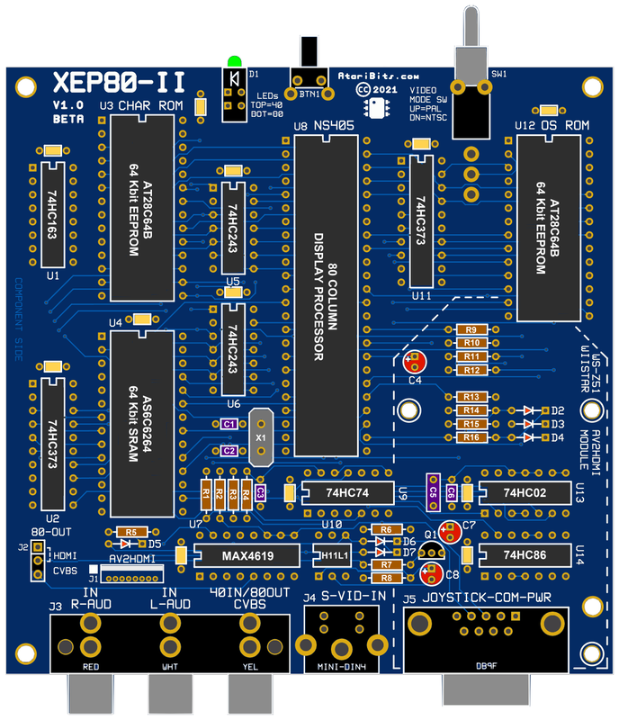
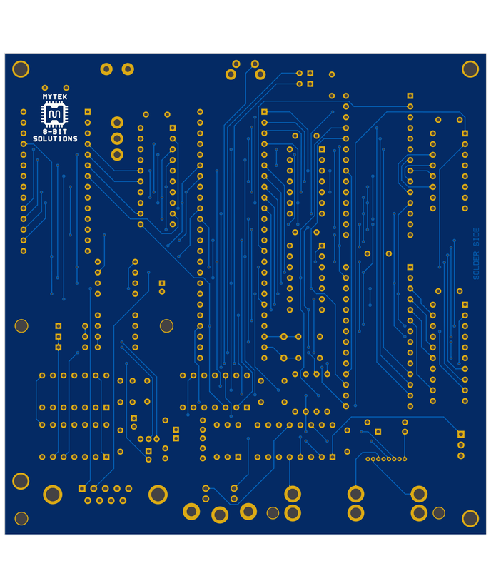
Let's pause for a minute and look at a preview image of the 'newest' 100% fully routed THT board layout. And for those that have been following this over at AtariAge, you'll possibly notice that I have moved the A/V-to-HDMI converter landing spot, so that it can now be flipped around 180 and have it's HDMI port facing the same direction as all the other jacks. This will become much more obvious when I post some pics of the real assembled boards.
The JST 1.25mm x 8-pin male connector (J1) is to provide connection to the optional Wiistar WS-Z51 A/V-to-HDMI converter. It requires a double-ended cable with 8-pin female JST connectors to mate the two aspects together. Once connected, the 80 column output can be sent thru the HDMI port. And the stock Atari 40 column text output (as well as graphics) can also be converted to HDMI, with either being individually displayed at the press of a button.
Jumper block header (J2) is for configuration without an A/V-to-HDMI converter daughter board being present, so that the 80 column composite signal can be routed directly out through the yellow RCA jack to feed a standard composite monitor instead.
The three RCA (J3) jacks on the left provide the following inputs from left to right: Right channel audio, Left channel audio, and composite video (CVBS). The Mini-DIN (J4) jack provides an S-Video input. These analog A/V signals are only required if the A/V-to-HDMI converter is installed, and will get sourced from the Atari's normal video output jack using a suitable A/V cable.
And last but not least we come to the DB9 jack on the far right which is to be connected to one of the Atari's joystick ports to provide both serial communication and 5 VDC power.
| |||
Over the next couple of weeks I will be testing the newer 74 series High Speed CMOS chips in place of the older 74LS ones originally found on the XEP80. I'll also be testing the new lower power display RAM, and the lower power EEPROMS that will take the place of the factory ROMs. This is all aimed at extracting power for this board from the Atari's joystick port without overwhelming the stock power supply. If all goes well and the board+schematic are brought to an error free state, I will then have a small batch of boards made by JLCPCB for testing.
Update: July 22nd 2021 - All of the chips in my stock XEP80 baseline unit were replaced with their 74HCxxx counterparts that were proposed for the new design, as well as the newer SRAM and EEPROMS. After this change, power draw dropped from 430 ma down to 210 ma, making it practical to derive power solely from the Atari, while XEP functionality remained unaffected. Gerbers have since been sent to JLCPCB for sample boards to be manufactured.
That pretty much covers it for now,
- Michael


 RSS Feed
