 C64-VGATE Main Video Board
 It's been a busy few weeks for me, so I wasn't able to post an update on this project until now.
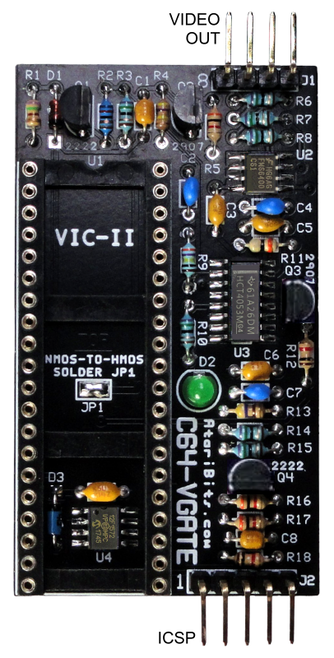
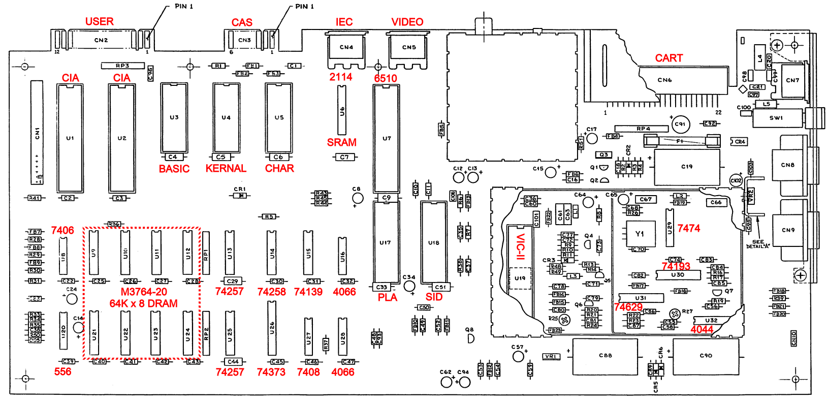
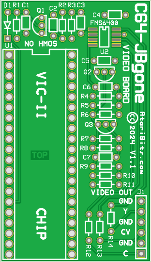
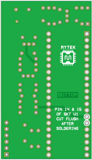
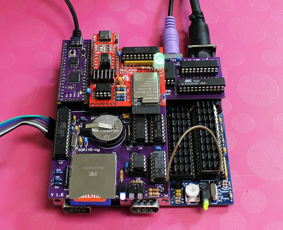
About 2 weeks ago I was able to assemble one board set with an HMOS 8562R4 VIC-II chip and installed it in my 250407 Long Board, using it's built-in NMOS-to-HMOS configuration jumper and special piggyback socket.
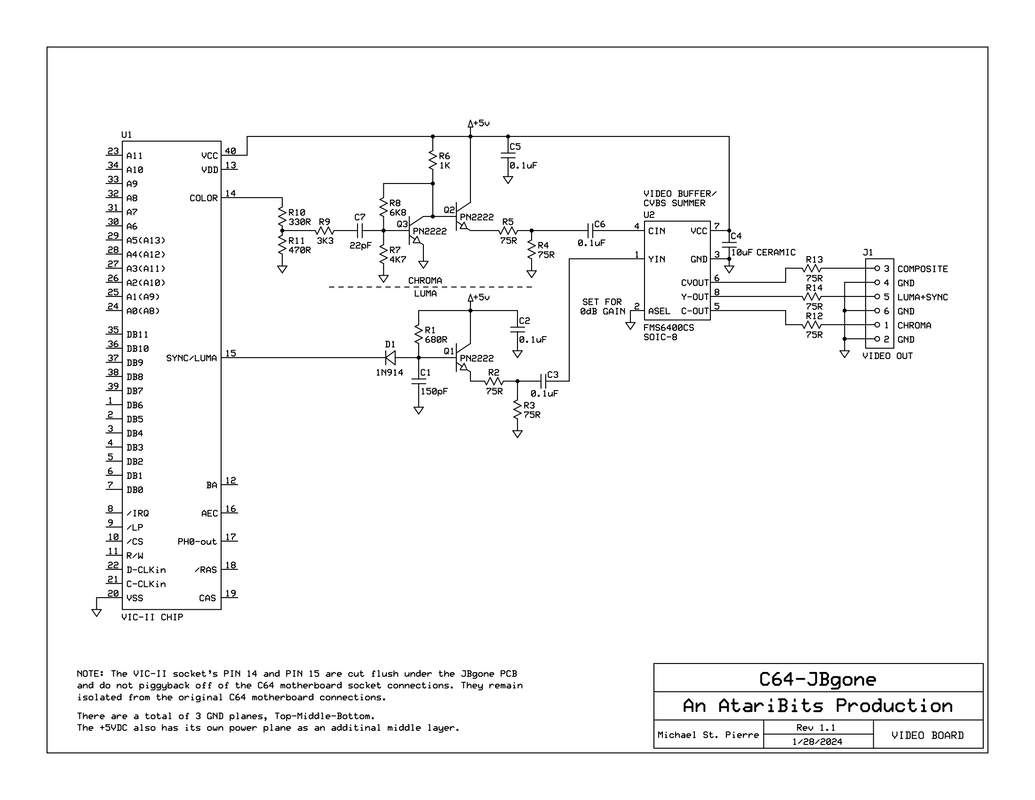
After some initial experimentation, I settled on what appeared to be the best component values, including figuring out a way to boost the video output all the way up to 1 V P/P without causing any shadowing when bright colors were being displayed, something that I had previously seen during earlier attempts to increase the video to that same level.
I was also able to compensate for some thermal drift issues that caused misalignment of the VGATE black level with the one generated by the VIC-II chip by changing out several resistors from 5% Carbon Film types over to 1% Metal Film types instead. Metal Film resistors have a much better temperature coefficient of resistance than carbon film types.
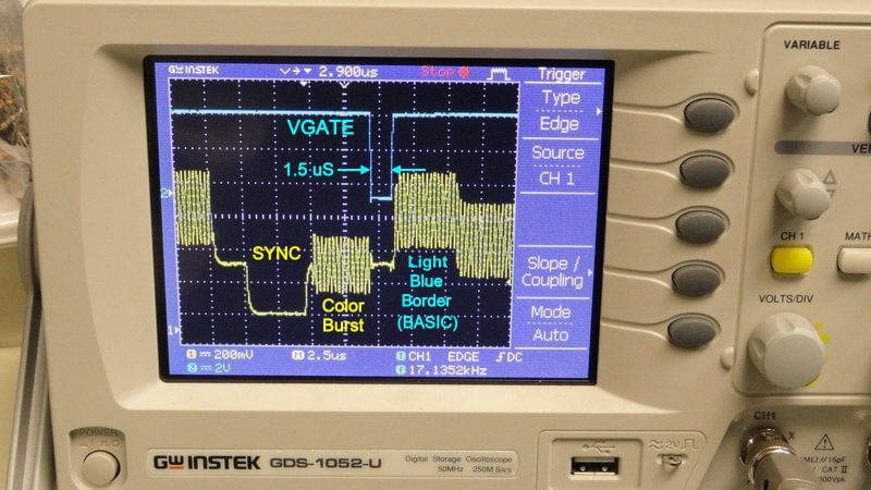
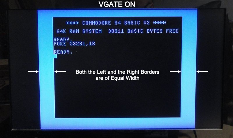
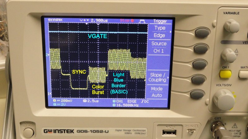
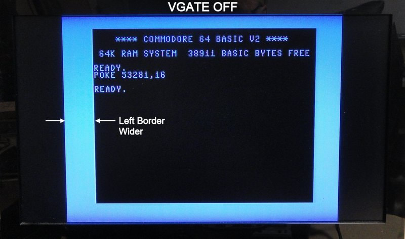
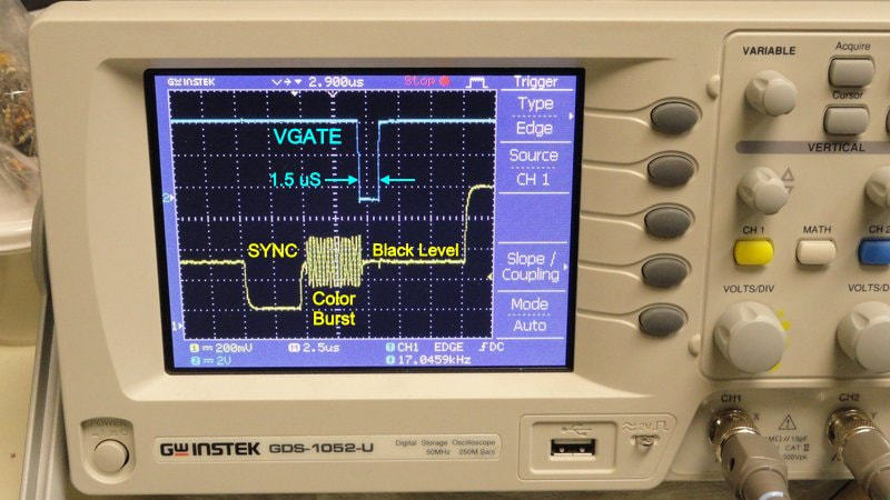
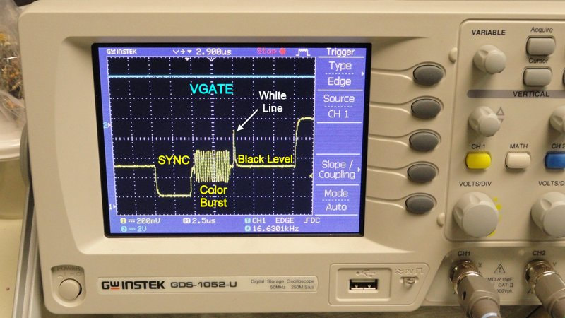
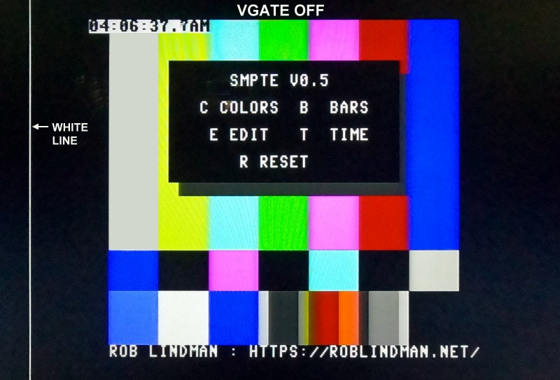
Overall the video output of the C64-VGATE video board is quite excellent, and the VGATE technology eliminates the white line that's usually seen on the left side of the image when viewed on newer HD monitors. However in order to achieve the best results it did require some additional timing adjustments in the VGATE firmware.
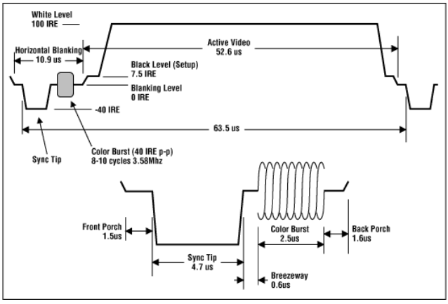
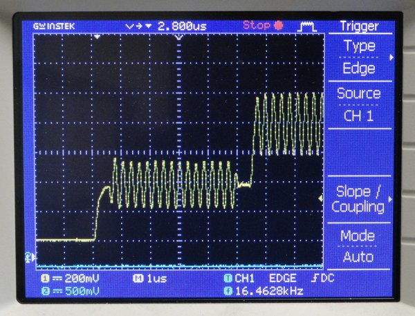
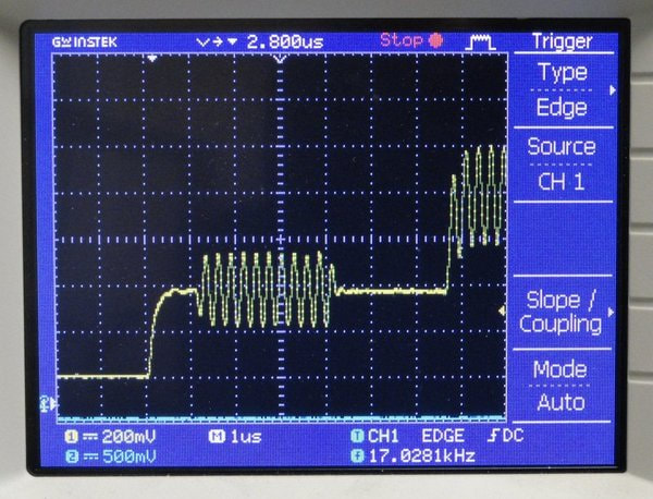
A nice side effect of eliminating the white line was that my cheap S-Video to HDMI converter was able to properly do the conversion without weird color and contrast issues it previously suffered from. I believe the reason for this improved behavior had to do with the white line causing confusion as to what the black level really was, because it occurred so soon after the color burst signal. With VGATE active, there now exists both a proper breezeway and back porch in the video output, something that was lacking in the original VIC-II output. And apparently my HDMI converter likes it much better.
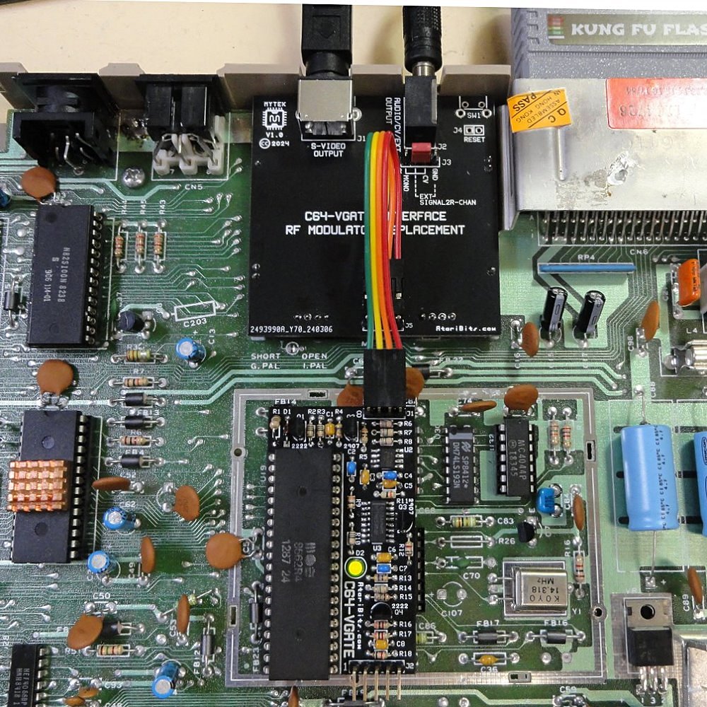
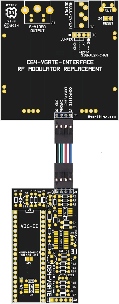
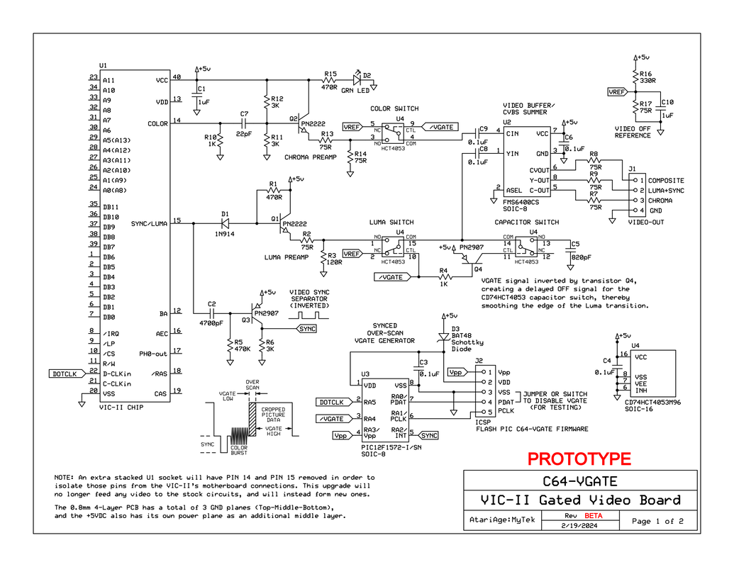
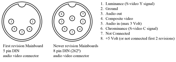
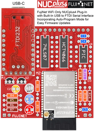
Keep in mind that this upgrade is much more than just the elimination of the white line. It's also meant to improve the video output quality utilizing triple shielding, a higher quality video output buffer, and by breaking out the S-video into a more standardized connection scheme. At the same time, there is also provision for stereo audio output, or composite video, or LumaCode video assuming the proper upgrades are also present. These last signals are broken out to a separate 3.5 mm jack, and with the addition of a simple RCA 'Y' adapter can be connected to standard RCA inputs.
Soon I'll be updating both the schematics and a download for the firmware reflecting these changes.
I also got some HMOS PAL VIC-II chips, so I should be able to see how this improved video system works for PAL as well.
Hopefully my next blog post will cover much more detail... stay tuned.
LINK to Previous Related Post.
-Michael
About 2 weeks ago I was able to assemble one board set with an HMOS 8562R4 VIC-II chip and installed it in my 250407 Long Board, using it's built-in NMOS-to-HMOS configuration jumper and special piggyback socket.
After some initial experimentation, I settled on what appeared to be the best component values, including figuring out a way to boost the video output all the way up to 1 V P/P without causing any shadowing when bright colors were being displayed, something that I had previously seen during earlier attempts to increase the video to that same level.
I was also able to compensate for some thermal drift issues that caused misalignment of the VGATE black level with the one generated by the VIC-II chip by changing out several resistors from 5% Carbon Film types over to 1% Metal Film types instead. Metal Film resistors have a much better temperature coefficient of resistance than carbon film types.
Overall the video output of the C64-VGATE video board is quite excellent, and the VGATE technology eliminates the white line that's usually seen on the left side of the image when viewed on newer HD monitors. However in order to achieve the best results it did require some additional timing adjustments in the VGATE firmware.
A nice side effect of eliminating the white line was that my cheap S-Video to HDMI converter was able to properly do the conversion without weird color and contrast issues it previously suffered from. I believe the reason for this improved behavior had to do with the white line causing confusion as to what the black level really was, because it occurred so soon after the color burst signal. With VGATE active, there now exists both a proper breezeway and back porch in the video output, something that was lacking in the original VIC-II output. And apparently my HDMI converter likes it much better.
Keep in mind that this upgrade is much more than just the elimination of the white line. It's also meant to improve the video output quality utilizing triple shielding, a higher quality video output buffer, and by breaking out the S-video into a more standardized connection scheme. At the same time, there is also provision for stereo audio output, or composite video, or LumaCode video assuming the proper upgrades are also present. These last signals are broken out to a separate 3.5 mm jack, and with the addition of a simple RCA 'Y' adapter can be connected to standard RCA inputs.
Soon I'll be updating both the schematics and a download for the firmware reflecting these changes.
I also got some HMOS PAL VIC-II chips, so I should be able to see how this improved video system works for PAL as well.
Hopefully my next blog post will cover much more detail... stay tuned.
LINK to Previous Related Post.
-Michael
Complete C64-Vgate Video Board Set Installed in Long Board 250407

 RSS Feed
